The ScienceDaily article from January 11, 2026, titled “This new imaging technology breaks the rules of optics,” details a breakthrough in Multi-Aperture Synthetic Imaging (MASI) developed at the University of Connecticut.1
While the article focuses primarily on a “software-first” approach to imaging, the implications for lithography (the process of “printing” circuits on chips) are significant, particularly in overcoming the physical and economic barriers of current nanomanufacturing:
1. Breaking the Diffraction Limit (Sub-micron Resolution)2
The technology creates a “virtual aperture” that achieves sub-micron resolution from distances previously thought impossible.3 In lithography, resolution is traditionally limited by the wavelength of light and the physical size of the lens (the diffraction limit). MASI’s ability to sidestep these physical limits suggests a path toward high-precision patterning without the need for increasingly massive and expensive lens systems.
2. Transition to Maskless and Lens-Free Systems
The research demonstrates ultra-sharp imaging without lenses or painstaking alignment.4
- Implication: Current Extreme Ultraviolet (EUV) lithography requires incredibly complex mirrors and lenses. A MASI-based approach could lead to lens-free lithography systems that are lighter, easier to maintain, and less prone to the aberrations caused by physical glass or mirrors.
3. “Software-Defined” Precision
The core of the breakthrough is using multiple sensors to collect raw light patterns independently and synchronizing them via computation rather than physical hardware.5
- Implication: This shifts the burden of precision from mechanical hardware to computational algorithms. In a lithography setting, this could allow for “software-defined” patterning where the light field is computationally reconstructed at the wafer surface, potentially reducing the need for physical masks (maskless lithography) which are currently one of the highest costs in chip production.
4. Scalability and Cost Reduction
The article highlights that the framework is “flexible and scalable.”6
- Implication: Current lithography machines (like those from ASML) cost hundreds of millions of dollars due to their scale and precision requirements. By using a scalable sensor/emitter array and computational synchronization, MASI could pave the way for smaller, modular, and significantly cheaper lithography tools, democratizing high-end semiconductor manufacturing.
5. Improved Metrology and Inspection
Beyond the printing process itself, MASI has immediate applications in wafer inspection. The ability to capture wide-field, high-resolution images from a distance allows for faster, more accurate detection of defects on a silicon wafer without the slow, “stitch-by-stitch” scanning required by traditional microscopy.
Summary: For the lithography industry, this technology suggests a future where computational optics replaces physical hardware, allowing for sub-micron chip manufacturing that is more flexible, cheaper, and no longer bound by the “rules” of traditional refractive optics.
While both technologies aim to achieve high resolution by combining signals from multiple small sensors to act as one large “virtual” sensor, Synthetic Aperture (SA) is a broad historical principle, whereas the Multiscale Aperture Synthesis Imager (MASI) is a specific 2026 technological breakthrough that solves the “optical barrier” that previously plagued SA.
The primary difference lies in how the sensors are synchronized and the wavelengths they use.
At-a-Glance Comparison
| Feature | Traditional Synthetic Aperture (SA/SAR) | Multiscale Aperture Synthesis Imager (MASI) |
| Primary Medium | Radio waves/Microwaves (Radar) | Visible Light / Optical |
| Hardware | Usually a single moving antenna or rigid array | Distributed array of static, independent sensors |
| Synchronization | Physical & temporal (requires nanosecond precision) | Computational (software-based phase alignment) |
| Physical Setup | Requires precise mechanical alignment or overlap | Flexible; sensors can be at different depths/locations |
| Lenses | Uses traditional antenna/optical focus | Lensless (captures raw diffraction patterns) |
| Key Limitation | Difficult to scale to optical due to tiny wavelengths | Requires heavy “software-first” processing power |
1. The Synchronization Challenge
- Traditional SA: To work, all sensors (or one moving sensor) must know their position relative to the light wave with extreme precision. For radio waves (centimeters long), this is manageable. For visible light (nanometers long), even a vibration the size of a bacteria ruins the image.
- MASI: Instead of trying to hold the sensors perfectly still or aligned, MASI lets them capture light “messily.”1 It then uses a computational phase synchronization scheme to fix the alignment in post-processing.2 It essentially “calculates” where the sensors were and how the light hit them.3
2. Lensless vs. Refractive Optics
- Traditional SA: In its optical forms (like the Event Horizon Telescope or Large Binocular Telescope), it still relies on complex mirrors or lenses to focus light before it hits the sensor.
- MASI: It is entirely lensless.4 It doesn’t look at an “image”; it looks at diffraction patterns (the way light scatters off an object).5 Because there are no lenses, it avoids common optical issues like chromatic aberration or the physical bulk of glass.6
3. Field of View and Working Distance
- Traditional SA: Often has a very narrow field of view when zoomed in for high resolution.
- MASI: Uses a “multiscale” approach.7 It can resolve sub-micron features (like the ridges on a hair) from ultralong distances (centimeters or meters away).8 Because it uses many sensors, it naturally expands the imaging field, creating a high-resolution view that is much larger than the sensors themselves.9
4. Scalability
- Traditional SA: Scaling up an optical SA system (like building a bigger telescope array) is exponentially more expensive because every new sensor must be physically integrated into a rigid, vibration-proof framework.
- MASI: Scales linearly.10 To get better resolution or a wider view, you simply add more cheap sensors to the array.11 The software handles the complexity, not the construction.12
Summary: If Traditional Synthetic Aperture is a “choir” that must sing in perfect, physical unison to be heard, MASI is a group of independent singers recorded separately and perfectly “auto-tuned” and synchronized by a computer afterward to create a symphony.13
Would you like me to dive deeper into the specific algorithms MASI uses to synchronize these phases without physical overlap?
In the video from Anastasi In Tech, the discussion centers on a startup called Substrate that is bypassing traditional Extreme Ultraviolet (EUV) lithography in favor of X-ray Lithography [07:12].
The primary distinction is that while MASI (from your previous source) uses a “software-first” computational approach to visible light to break optical rules, X-ray Tomography/Lithography relies on a fundamentally different, much shorter wavelength of light to achieve sub-nanometer precision [00:21].
Key Comparisons between X-ray Lithography and MASI
| Feature | X-ray Lithography (Substrate) | MASI (UConn Breakthrough) |
| Light Source | Compact Particle Accelerator [11:36] | Standard Visible Light/Sensors |
| Wavelength | 0.1 to 10 nm (Anstrom era) [08:52] | Visible spectrum (Software-enhanced) |
| Method | “Stamp” the entire drawing in one shot [08:43] | Computational reconstruction of patterns |
| Cost | ~$50M per tool (vs $500M for High-NA EUV) [13:42] | Low-cost sensor arrays / High-end compute |
| Industry Aim | Building entirely new chip factories [00:35] | General sub-micron imaging & metrology |
1. The Light Source and Wavelength
- X-ray: Uses electromagnetic radiation with wavelengths up to 1,000 times shorter than EUV [09:01]. To do this inside a factory, they use a “compact particle accelerator” where electrons are wiggled via magnetic structures to emit X-rays [12:03].
- MASI: Operates on the principle of Multi-Aperture Synthetic Imaging, using software to overcome the diffraction limits of visible light rather than changing to a more “difficult” light source like X-rays.
2. Single Exposure vs. Multi-Patterning
- The video highlights that current EUV requires “multi-patterning”—splitting patterns into multiple passes like drawing with a marker that is too thick [04:45].
- X-ray Lithography aims for single-shot exposure of sub-nanometer features [00:21], drastically reducing the complexity and defect risk associated with multiple passes [12:50].
3. Material Challenges
- A major point in the video is that X-rays pass through most materials instead of bending [09:12]. This requires Substrate to reinvent the photoresist (the light-sensitive chemistry) and the masks themselves, because the materials used for UV simply don’t work for X-rays [14:20].
- MASI faces fewer material hurdles since it uses standard optical sensors but requires immense computational power to synchronize the “phase” of light patterns captured by different sensors.
4. Economic Disruption
- The video suggests that X-ray tools could cost $50 million, a tenth of the cost of ASML’s $500 million High-NA EUV machines [13:42].
- This is similar to the MASI implication: both technologies aim to “democratize” high-end manufacturing by shifting the cost from massive, near-perfect physical optics to more manageable hardware (either compact accelerators or sensor arrays) [17:54].
Summary: While MASI is a breakthrough in how we process light to see small things, the X-ray technology described in the video is a breakthrough in the physical tool used to print them. Both, however, represent a shift away from the “incremental steps” of the current semiconductor industry toward a more radical, “physics-defying” future [00:46].
Integrating Multi-Aperture Synthetic Imaging (MASI) with X-ray lithography (like the system from Substrate) offers a powerful “hardware + software” synergy. While X-rays provide the raw physical resolution to print at sub-nanometer scales, MASI provides the computational “eyes” to ensure those patterns are perfect in real-time.
1. Real-Time “In-Situ” Error Correction
The biggest challenge in X-ray lithography is that X-rays are notoriously difficult to focus or steer with traditional lenses.
- MASI’s Role: Because MASI is lens-free and relies on an array of sensors to reconstruct images from diffraction patterns, it can be integrated directly into the lithography chamber.1
- Application: It can monitor the X-ray “printing” process as it happens. If the software detects a nanometer-scale shift due to thermal expansion or vibration, it can feed that data back to the X-ray source’s steering magnets to compensate instantly.
2. Overcoming “Penumbral Blur”
In X-ray lithography, a common error is “penumbral blur”—a slight fuzziness at the edges of a feature caused by the finite size of the X-ray source.
- Correction: MASI is specifically designed to resolve features smaller than the physical limits of the imaging hardware.2 By using MASI to image the printed resist, the system can use deconvolution algorithms to mathematically subtract the blur from the inspection data, giving engineers a “true” view of the printed nanostructures that a traditional microscope would miss.
3. Mask Alignment and Distortion
X-ray masks are often made of thin membranes that can warp under the intense energy of a particle accelerator.
- Digital Correction: MASI can create a “virtual aperture” that is much larger than any single sensor. This allows it to capture a wide-field, high-resolution map of the entire mask.
- Result: It can detect sub-micron distortions across the whole mask surface simultaneously. This “distortion map” is then used to digitally adjust the X-ray pulse timing or the wafer stage position to “print around” the physical errors in the mask.
4. Metrology Without the “Wait”
Currently, wafers often have to be moved to a separate Electron Beam (e-beam) tool for inspection, which is slow and breaks the vacuum.
- MASI Advantage: MASI provides optical-speed metrology with e-beam-like resolution. It allows for “Through-the-Lens” (or in this case, Lensless) inspection. This means errors are caught after the first few nanometers of exposure rather than after the entire wafer is finished, saving millions in wasted silicon.
Comparison of Error Correction Methods
| Error Type | Traditional Correction | MASI-Enhanced X-ray |
| Vibration | Heavy lead shielding/Damping | Real-time computational re-alignment |
| Mask Warp | Physical cooling systems | Digital mask compensation (Software) |
| Edge Blur | Shrinking the light source | Computational deconvolution |
| Defect Detection | Post-process SEM (Slow) | In-process MASI Metrology (Fast) |
A technical diagram showing how a MASI sensor array would be positioned relative to an X-ray source and wafer:
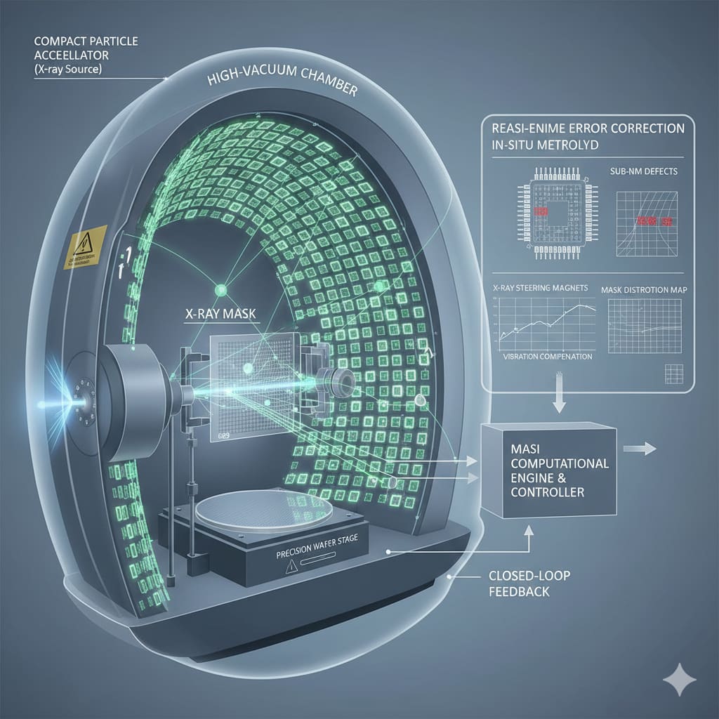
X-Ray Lithography: The Future of Chip Manufacturing
This video explains the mechanics of X-ray lithography and the specific challenges—like mask distortion and precision—that MASI technology is designed to solve.
Sources
New Image Sensor Breaks Optical Limits – UConn Today